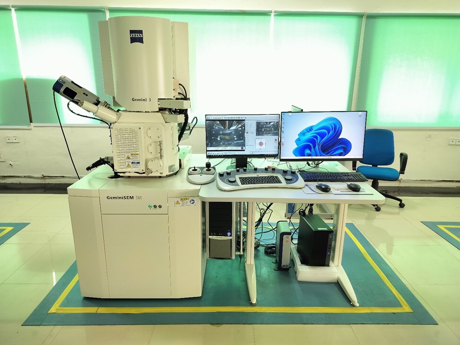
Field Emission Scanning Electron Microscope (ZEISS Gemini 560)
About Instrument and its applications -
Gemini 560 FE-SEM equipped with Oxford EDS provides topographical and elemental information of different types of samples at magnifications from 10X to 10,00,000X. It has good spatial resolution (~ 0.5 nm) to cater the research needs of the different departments of IIT Roorkee and various external users.
General Information-
Make- Carl Zeiss, Germany
Model- Zeiss Gemini 560
Year of Installation- 2024
Specifications-
1) Source: High brightness field emission electron source (Schottky FEG)
2) In-lens SE and In-lens BSE detector
3) Retractable high efficiency 5 sector annular BSE detector
4) ET SE detector
5) Color CCD Camera
6) Resolution: ~ 0.5nm at 15 kV, ~0.8nm at 1 kV
7) Magnification: 10 – 10,00,000X
Sample Requirements and preparation-
Solid Samples:
1) Cut the solid sample into smaller, manageable pieces.
2) Clean the sample surface using an appropriate solvent or ultrasonic cleaning to remove contaminants. Metallic samples need to be polished and etched. Ensure the sample is completely dry.
3) Place a small piece of conductive double-sided tape on the stub. Affix the solid sample onto the tape, ensuring secure adhesion.
4) Apply a thin conductive coating (e.g., gold or palladium) to enhance conductivity, especially for non-conductive materials, if required.
Powder Samples:
1) Place a small amount of the powder sample onto a piece of conductive double-sided tape.
2) Gently press down on the powder to create a flat surface for imaging.
3) Apply a thin conductive coating to enhance imaging quality, especially for non-conductive powders, if required.
Biological Samples:
1) Fix biological samples using suitable fixatives like formaldehyde or glutaraldehyde to preserve cellular structures.
2) Gradually dehydrate the sample using a series of ethanol solutions or other dehydration agents.
3) Perform critical point drying to replace the liquid solvent with a gas, avoiding damage to delicate structures.
4) Place the dried sample onto a piece of conductive double-sided tape on the stub, ensuring secure adhesion.
5) Apply a thin conductive coating to enhance imaging quality.
Nanomaterials Dispersed in Liquids:
1) Disperse nanoparticles or nanotubes in a suitable solvent to create a well-dispersed solution.
2) Deposit a small amount of the dispersed solution onto a conductive substrate for imaging. Allow solvent evaporation.
3) Mount the substrate with the deposited nanomaterials onto a stub using conductive tape.
4) Ensure the sample is completely dry, and solvent residues are removed.
5) If required apply a thin conductive coating to enhance imaging quality, especially for non-conductive nanomaterials.
Contact Person-
Dr. Shriniwas Yadav
Technical Officer-II
E-mail: shriniwas.mic@iitr.ac.in
Tel: +91-1332-284560