DEPARTMENT OF ELECTRONICS AND COMMUNICATION
INDIAN INSTITUTE OF TECHNOLOGY ROORKEE
Microelectronics Lab
Alt text
Alt text
Alt text
Alt text
About

The Microelectronics Laboratory, under the Department of Electronics and Communication Engineering, is a dedicated research facility for PhD students actively work across diverse domains of microelectronics. This lab is also used as part of UG and Master Curriculum for training of semiconductor fabrication and characterization. The lab is equipped with state-of-the-art instruments that enable the fabrication of a wide range of devices, including:

• Transistors
• MEMS
• Sensors
• Solar Cells
• 2D Devices
• Thin-film deposition
• Organic Opto-electronic devices.
Alt text
Microtech LW-405

An Optolithography technique in which a laser beam/ LED is used to form the desired patterns on the photoresist is called laser /LED writing (Direct writing).
Lithography is a critical process in microfabrication, enabling the precise patterning of substrates for semiconductor, MEMS, and nanotechnology applications. Laser writer lithography utilizes a focused laser beam to expose a photoresist-coated substrate directly, offering high-resolution patterning without the need for masks.
This technique is essential for rapid prototyping and research applications where flexibility and precision are paramount.
PRECISION PROGRAMMABLE SPIN COATING SYSTEM (Model: SpinNXG-P2)

Laurell Spin Processor is used to distribute Photoresist in a uniform layer by spinning a Substrate.
Applications
• Micro-fabrication of Oxide Layers.
• Nano-scale & Micron-scale Uniform & Homogeneous Thin Film Preparation.
• Preparation of Photo-resist Layers for Photolithography & for defining Patterns in Micro-circuit Fabrication.
• Dielectric / Insulating Layers for Microcircuit Fabrication, Flat Screen Display, Anti-reflection, Magnetic Disk, CD, DVD & CD ROM Coatings.
• Magnetic Particle Suspensions, Head Lubricants, Conductive Oxide Coatings Television Tube Phosphor and many more.
Alt text
Alt text
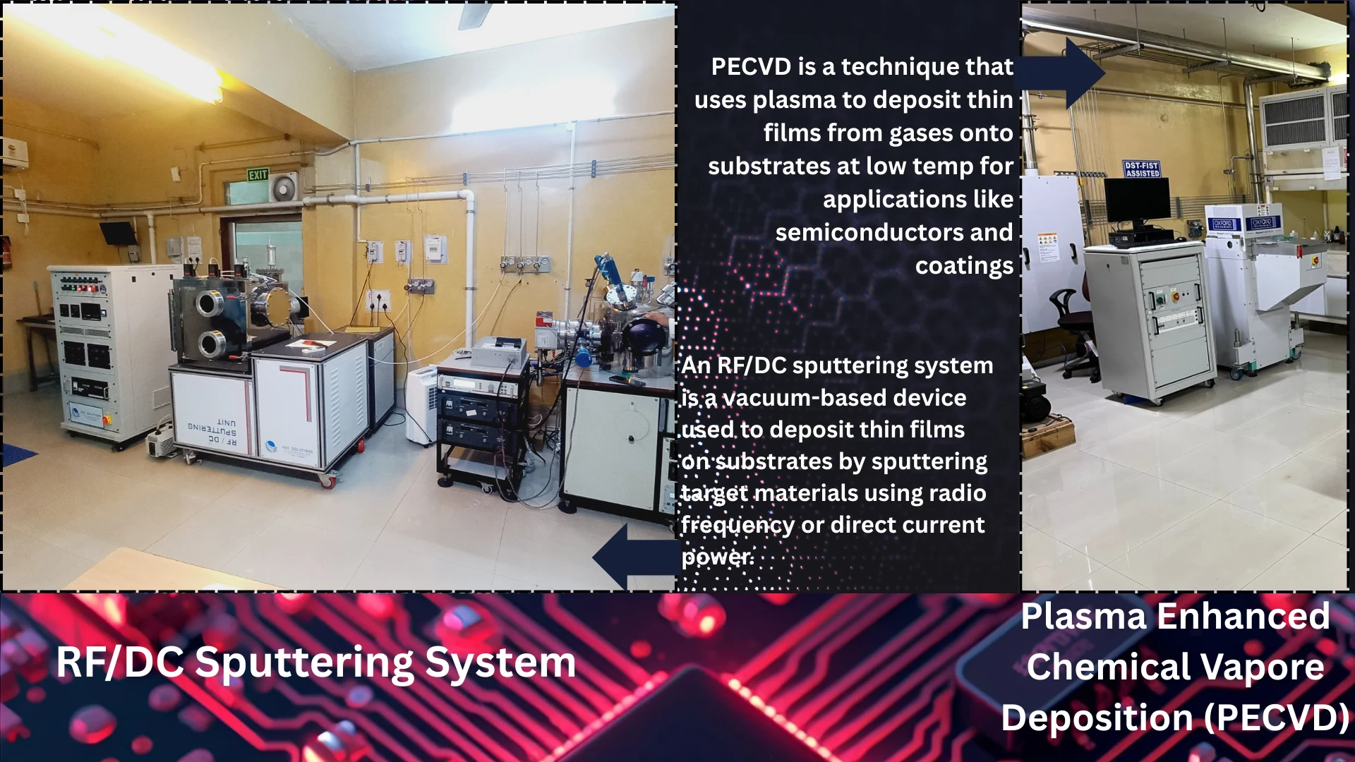
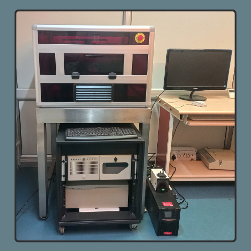
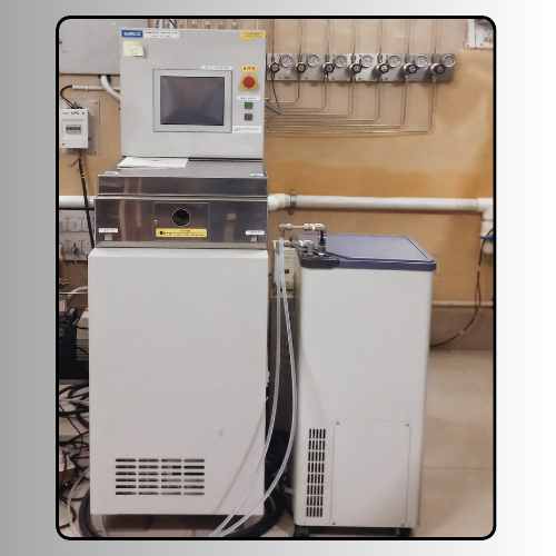
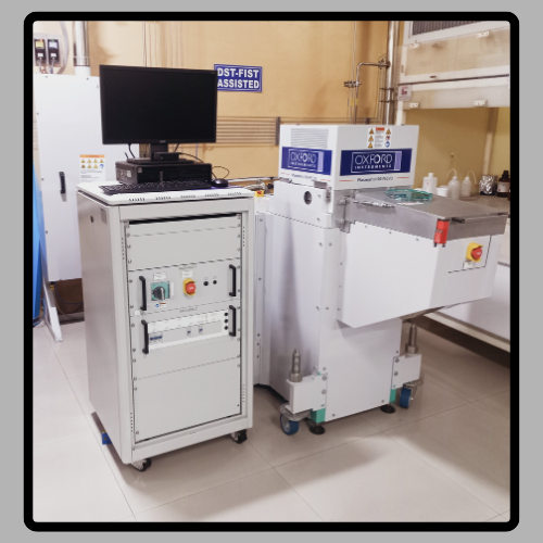
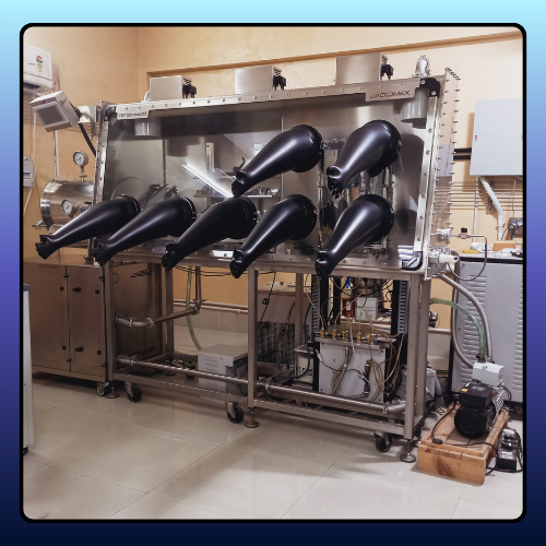
SAMCO RIE-10NR Reactive Ion Etch System:

Reactive Ion Etching (RIE) is an etching technology used in micro and nano fabrication wherein plasma is used to remove materials deposited on the substrate. Plasma is generated under low pressure by electromagnetic field. High energy ions from the plasma attack the wafer surface and react with it to remove the film. Plasma Reactive Ion Etching System is a Reactive Ion Etching tool from SAMCO Instruments.

Applications
• Highly controllable anisotropic etching of a variety of materials, including semiconductors (e.g., crystalline, polycrystalline oxides, 2D Transition-metal dichalcogenides, etc.), dielectrics (e.g., oxides, nitrides, etc.) and metals (e.g., Poly-Si, conducting oxides, Au, TiN, including refractory metals, Mo, W, etc.) as well as carbon-based materials (e.g., graphene, MXenes, etc.).
Chemical Wet Bench Acid Clean:

• Chemical wet bench Acid clean is used for cleaning of unprocessed, new cut pieces to full 4 inch Si wafers.
• RCA/piranha of non-preprocessed (new) & wafers going into First nano furnaces, oxide and oxynitride etch of samples.
• Quartzware and PP petridishes for processing substrates.
Alt text
Alt text
Sputter Deposition:

Sputtering is a widely used Physical Vapor Deposition (PVD) technique for depositing thin films onto substrates. It involves bombarding a target material with high-energy ions (typically argon), causing atoms to be ejected and deposited onto a substrate. Sputtering is extensively used in semiconductor manufacturing, optical coatings, and protective layer applications due to its superior film adhesion, uniformity, and material versatility. Our system in the lab is a three-target system where three metals/dielectric materials can be sputtered without breaking the vacuum.

Vacuum Coating unit model 12A4-D (Hind Hivac system)/ Electron Beam Evaporation:

A stream of high energy electrons heats up the source to generate vapors that condense onto a substrate to form a thin film. HHV provides electron guns from single pocket to multi pocket sources with large capacity for a range of applications from R&D to multi-layer depositions that require higher film thicknesses.

Applications:

To produces thin, homogenous, uniform, pure film coatings of various metals to achieve controlled effects in applications like optics, electronics, materials, thin film coating etc.
Alt text
Alt text
Thermal Evaporator

Thermal Evaporator system capable of evaporating a wide variety of materials, including organic, inorganic, and metal. In this thermal evaporator vacuum is achieved with the HHV Hi-Vac system and customized electronics for automatic feedback control of deposition rate
PlasmaPro 100 PECVD

Plasma Enhanced Chemical Vapour Deposition (PECVD) utilizes plasma to enhance the reaction of the precursors. It is a low temperature process when compared to conventional Chemical Vapour Deposition (CVD). It uses RF energy to generate plasma where the deposition can be done below 380C. The deposited material will be conformal in nature. The deposition rate is high compared to conventional CVD. The deposited material can have smooth surface. The deposited material will always be amorphous in nature. PlasmaPro 10 PECVD System is a deposition tool from Oxford Instruments.

Applications:
• High quality PECVD of Dielectric materials like SiOx, SiNx, SiOxNy, GeOx for photonics, dielectric layers, passivation and many other uses.
• Semiconductor materials like a-Si, Ge, SiGe can be deposited.
• Phosphorus and boron doped oxide films can be deposited.
• Stoichiometry of the deposited material can be controlled.
• Film stress can be controlled by high/low frequency mixing techniques.
Alt text
Alt text
Oxidation Furnace

A manual tube furnace is used for wet and dry oxidation of wafers. The Oxidation Furnace (Dry) can create a layer of Oxide on silicon or glass wafers.Processes (Dry Oxidation)
• Thermal Oxidation
• Has a lower rate of oxide growth, but a better film quality
• Used for making thin oxides.
• Gases available are oxygen and nitrogen.
• Temperatures up to 1150 deg C.

Processes (Wet Oxidation)

• Wet oxidation uses pure steam for oxidation
• Has a significantly higher rate of growth compared to dry oxidation
• Used for making thicker oxides like field oxide
• Gases available are Oxygen and Nitrogen
• Temperatures up to 1150 deg C


Annealing Furnace

An annealing furnace is a laboratory equipment used to heat samples to a controlled temperature and then cool them at a defined rate. The process of annealing improves material properties such as crystallinity, conductivity, and mechanical stability by relieving internal stresses and promoting structural reorganization. The furnace allows precise control over temperature, heating duration, and atmosphere (air, inert gas, or vacuum), making it an essential tool for material processing experiments.
Alt text
Alt text
Rapid Thermal Anneal system (RTP)

The MILA-5000 Rapid Thermal Annealer is a laboratory system designed for high-speed heating and cooling of samples under controlled environments. It uses a halogen lamp-based heating mechanism to achieve precise temperature control up to very high ranges within a few seconds, enabling rapid thermal annealing (RTA) of thin films, semiconductors, and nanomaterials. The system allows processing in various atmospheres such as air, vacuum, or inert gases, making it versatile for material modification studies.
Profilometer: Dektak XT Stylus Profiler

The DektakXT Stylus Profiler is capable of quickly and accurately measuring feature heights on a surface. It can resolve step heights as small as 10nm. Variable force and measurement length settings make measurements possible on a wide range of materials and structures without damaging them. A magnified video targeting system permits positioning the needle tip near small surface features.

Applications
It is common to use a profilometer to measure film thickness and surface texture. Examples include thickness measurements made after spin coating or magnetron sputter deposition and height measurements that are used to calibrate the thickness monitor on a deposition system materials such as semiconductors, polymers, metals, and ceramics are commonly measured using this instrument.
Alt text
Alt text
Ocean Optics NanoCalc DUV Spectroscopic Thin Film Measurement

The Ocean Optics NanoCalc DUV Spectroscopic Thin Film Measurement tool utilizes spectroscopic reflectometry to accurately determine the thickness and optical parameters of thin films.
Wedge Bonder – West Bond 747677E

The wire bonder is a wedge-to-wedge ultrasonic bonder designed to interconnect wire leads to semi-conductor, hybrid, or microwave devices. Bonds are made by the wedge-wedge technique using ultrasonic energy to attach aluminum wire at room temperature and adding work piece heat for gold wire. Wire is clamped and threaded diagonally under the bonding wedge, allowing independent feeding action but requiring front-to-back bonding direction. The bonding tool is guided manually by the operator using hand/eye reference to bond targets and elevations.
Alt text
Alt text
Glovebox for working under inert conditions (GP Concept, Jacomex)

This glove box is aimed to develop processes sensitive to oxygen and water in an environment of nitrogen. The nitrogen of the box is constantly purified to eliminate contaminant traces produced during the processes. Glovebox is high performance purification unit maintaining low containment of oxygen and air moisture (<1 ppm), it is also equipped with purification unit for organic solvents which allows working with volatile solvents.
Probe Station and Parameter Analyser

A probe station is an interface tool to measure the electrical characteristics of microelectronic device. By using a combination of a microscope and micropositioners, users can accurately make contact with probes to touch onto their device and use other electronic meters to see their results.
The Probe Station facilitates electrical measurements at room temperature and in ambient conditions. Electrical contact is made via probe tips (5 µm tungsten standard) which are attached to micropositioners with 80 turns per inch resolution. The electrical signals are taken through the Keithley 4200A-SCS Parameter Analyzer which has 4 SMU units with a DC current range of 10aA-1A and voltage range of 0.2μV-210V. The parameter analyzer delivers synchronizing temperature-dependent current-voltage (I-V), capacitance-voltage (C-V), and ultra-fast pulsed I-V measurements.
Alt text
Contact Us

Dr. Sanjeev Manhas
Dr. Arnab Datta
Department of Electronics & Communication
Indian Institute of Technology Roorkee
Haridwar Highway, Roorkee,
Uttarakhand 247667